PCIe Carriers & Digitizers
PCIe FMC Signal Processing Carrier
Half-length PCIe carrier for one FMC or FMC+ module
Host interface
PCIe Gen2 x8 / Gen3 x8
Throughput
Up to 3.6 GB/s
FMC site
VITA 57.1 / 57.4
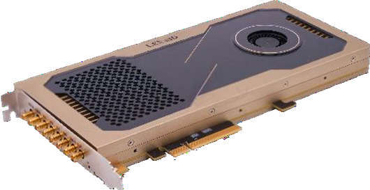
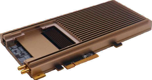
PCIe FMC signal processing carrier: a Kintex-7 or Virtex-7 class FPGA, on-board DDR3, one FMC/FMC+ site and a PCIe Gen2 x8 or Gen3 x8 host interface. Two build options cover mainstream and high-throughput needs.
Typical response within one business day.
Drag to rotate · scroll to zoom
Interactive 3D view. Representative layout generated from the
datasheet dimensions — use it to check connector placement and mechanical
context, not for CAD fit. STEP models are available on request.
Specifications
Full specifications
| **PCIe Gen2 FMC** / **PCIe Gen3 FMC+** | |
| FPGA | XC7K325T or XC7K410T / XC7VX690T |
| Memory bank 1 | 64-bit DDR3, 2 GB / 64-bit DDR3, 2 GB |
| Memory bank 2 | 64-bit DDR3, 2 GB / 64-bit DDR3, 4 GB |
| FMC site | VITA 57.1 / VITA 57.4 |
| Host interface | PCIe Gen2 x8 / PCIe Gen3 x8 |
| Sustained throughput | 2 GB/s / 3.6 GB/s |
| Power | 30 W / 50 W |
| Reference clock | 1 x SSMA external reference input |
|---|---|
| Timing input | 1 x SSMA (IRIG-B compatible) |
| Auxiliary I/O | J30J-37: 4 x SPI, 2 x RS-232, 2 x RS-422, 4 x GPIO |
| Debug | 16-pin debug header |
| Power input | 12 V via PCIe slot |
|---|---|
| Dimensions | 233.33 x 126.30 x 21.59 mm |
| Operating temperature | -40 C to +55 C |
| Driver support | Windows, Linux |
Specifications subject to change without notice. Operating temperature ranges are the tested commercial ranges for the standard build.